Transistor
In 1947 John Bardeen, William Shockley, and Walter Brattain invented the transistor.
The most common of the various forms of transistors is the Bipolar Junction Transistor or BJT. It is a semiconducting device with three terminals or junctions. Junction diodes are mainly used for rectification of electrical signals. On the other hand, transistors are mainly used for electrical signal amplification. Most modern technology uses transistors; That is why semiconductors are so important today.
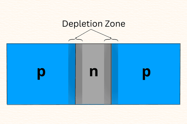
Transistors, like diodes, are made from a crystal. Transistors are tiny and sealed within a metal or plastic casing so as not to be exposed to air or water vapor. Transistors are of two types: 1. p-n-p transistor, and 2. p-n-p transistor.
Structure of a p-n-p transistor
- A thin n-type layer is doped between two p-type regions at either end of a semiconductor crystal. This thin n-type layer in the middle is much less thick than the two p-type regions on either side. This middle layer is called the base of the transistor.

- The two p-type regions at either end are called the emitter (E) and collector (C) of the transistor, respectively. Although these two regions appear similar, their levels of doping differ. The emitter region is more heavily doped than the collector. Hence, switching the emitter and collector connections in a circuit disrupts the operation of the transistor. The base doping level of the transistor is less than that of both the emitter and the collector.
- The majority charge carrier of this transistor is a hole. Generally, the hole is discharged from the emitter and passes through a thin layer of base to be received by the collector. A thin layer of soil controls the flow of these holes.
Structure of a n-p-n transistor
The structure of the n-p-n transistor is almost identical to the structure of the p-n-p transistor above. Only the doping properties of different parts of the semiconductor crystal are opposite.
- The middle thin base layer is p-type.
- The emitter and collector layers at both ends are n-type.
- The majority charge carriers for this type of doping are electrons.
Electrons are faster than holes as carriers. Hence, the n-p-n transistors are used in high-frequency and computer circuits. The faster the carriers are activated after sending the signal in such a circuit, the faster the work is done.
Circuit symbol
The symbols used to denote p-n-p and n-p-n transistors are respectively shown in the figure. The arrow indicates the direction of current flow between the emitter and base. Hence, the flow of electrons takes place against the direction of the arrow.

Transistor in an open circuit
As can be seen, two diodes are connected to form a transistor. Thus, just as a p-n junction diode is formed, the diffusion of electrons and holes across the junction is similar to that of a transistor. This causes each p-n junction to become reverse-biased without any external source. The depletion region is formed in this case as in the p-n junction diode.

Common-Emitter or CE configuration of a transistor
Three types of circuit connections can be made with transistors: 1. Common-base or CB, 2. Common-emitter or CE, and 3. Common-collector or CC. Among these, the common-emitter or CE circuit is most commonly used as an amplifier circuit.
How the CE circuit is constructed using an n-p-n transistor is shown in the figure. In this case, 1. The circuit connecting the base and emitter (leftmost circuit in the figure) is used as the input circuit and 2. The collector and emitter junction circuit (the rightmost circuit in the figure) is used as the output circuit. That is, the emitter is common to both circuits. In the alternating current circuit, this emitter is grounded. Hence, it is also called a grounded emitter circuit.

Biasing of a CE circuit
- Ground in the input circuit is forward-biased with the emitter connected to the base, i.e., the p-type base of the n-p-n transistor is connected to the positive terminal of the source-battery VBB.
- The collector of the output circuit is reverse-biased with the emitter connected to the base, i.e., the n-type collector of the n-p-n transistor is connected to the positive pole of the source-battery VCC.
Incidentally, the above bias arrangement is the condition for the transistor to be in the active state. But sometimes, it is kept in a different bias.
Current in CE circuit
In the input circuit, the emitter is at a negative potential concerning the base, so a large number of electrons are discharged from the emitter and attracted by the positive base. Since the base layer is very thin, most of these moving electrons penetrate the base layer and enter the collector, and are attracted by the positive potential of the collector. The few electrons that remain in the base are again attracted by the positive potential of the base. Thus, the electron flow in the emitter is divided into two parts:
- Base current of the input circuit,
- Collector current of the output circuit.
The conventional direction of current flow is opposite to electron flow; accordingly, the above figure shows the direction of emitter current IE, base current IB and collector current IC.
Clearly, IE = IB + IC
The value of IB is very low compared to IE or IC, about 1 in 100 to 500.
For example, If IB = 10 µA, IC = 2 mA = 2000 µA,
IE = 2000 + 10 = 2010 µA
CE characteristics
In the figure, input circuit voltage = VBB, output circuit source voltage = VCC.
Base flow, IB = input flow; base-emitter voltage, VBE = Input Voltage.
collector current, IC = output current; collector-emitter voltage, VCE = output voltage.
Input and output currents and voltages can be easily and arbitrarily changed. Input current IB and output voltage VCE; That is, IB and VCE are independent variables in the CE circuit. VBE and IC are dependent variables on these two. VBE is not particularly important in circuit analysis. So, the important relation is,
IC = f(IB, VCE) …….(1)
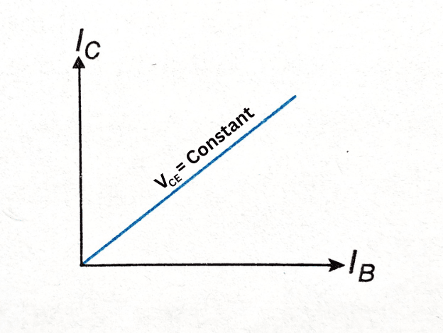
Using this (1)-number mathematical relationship, two types of CE circuit characteristic curves can be drawn.
Transfer characteristics
The curve obtained from IC concerning IB by keeping VCE constant is called the transfer characteristic. Because in this case IB and IC are the input and output quantities respectively.

Output characteristics
The curve of IC versus VCE obtained by keeping IB at various fixed values is called the output characteristic. Because, in this case, both VCE and IC are output quantities. A class of different output characteristics is available for different values of IB. This category is divided into three distinct regions:

Active region: In this region, the base-emitter junction is forward-biased and the collector-emitter junction is reverse-biased. Hence, IB > 0 and VCE > 0; However, in practice, the value of VCE needs to be greater than about 0.2 V to keep the collector junction properly reverse-biased. For a transistor to be used as an efficient current amplifier, its operation must be restricted to the active region.
Cut-off region: Both base-emitter and collector-emitter connections are reverse biased in this region.
Saturation region: Both base-emitter and collector-emitter connections are forward-biased in this region. Also, note that the collector is effectively forward-biased when the value of VCE is less than about 0.2 V.
Use of transistor as a switch
Any ideal switch when turned ‘on’ creates a closed circuit, while when turned ‘off’ creates an open circuit. Apart from that, this ideal switch can be switched from ‘off’ to ‘on’ state, or from ‘on’ to ‘off’ state with almost no time wasted.
No transistor can properly fulfil these conditions of an ideal switch. Nevertheless, transistors are widely used as fairly effective switches in various practical electronic circuits.
When a transistor is placed in the common-emitter junction system, the base-emitter junction is reverse-biased in the cut-off region. In this condition the ground current IB becomes negative and the value of the collector current IC becomes negligible. This is called the ‘off’ state of the transistor. On the other hand, when the ground current IB reaches a high positive value, the collector-emitter junction is forward biased and the transistor is placed in its saturation region. In this case, the collector-emitter voltage VCE is almost zero. As a result, almost all of the external bias VCC behaves as a threshold voltage across the load resistor RL. Hence the collector current IC also reaches quite high values. This state is considered as the ‘on’ state of the transistor.
Difference between transistor switch and standard switch
In a switch system, the base current of the transistor must be moved very quickly from positive to negative, or from negative to positive. This causes the transistor to switch from ‘on’ to ‘off’, or from ‘off’ to ‘on’ respectively. However, it takes some time for the collector current to reach IC high when turned ‘on’, or for the accumulated charge to decay to base when turned ‘off’. Hence, transistor switches can never operate at the speed of standard switches. Its efficiency can be increased only slightly by using some specially designed transistors.


Pingback: Oscillator - ASTRONOMY ADVENTURE
Pingback: Binary System - ASTRONOMY ADVENTURE