Conduction of electricity in solids
The molecules or atoms of crystalline solids are arranged in a regular pattern in a three-dimensional space. This design is called a lattice. Any lattice has the smallest structure, called a unit cell. Numerous small single cells are regularly arranged to form fragments of a crystal.
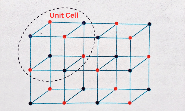
On the other hand, when the atoms of a solid are arranged randomly instead of in a regular pattern, an amorphous solid is formed. Solids can be divided into three categories based on the properties of electrical conductivity—1. Conductors, 2. Insulators, and 3. Semiconductors.
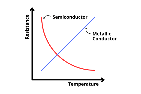
Conductors: Current can easily flow through conductors. A solid conductor is a metal. Free electrons mediated by metals act as charge carriers. Resistance of metallic conductors increases as temperature increases—for example, Copper, Silver, Aluminum, Iron, etc.
Insulators: Materials through which no current can flow at all are called insulators. No free electrons exist in them. Most nonmetals are insulators. Insulators commonly used in electronics are mica, diamond, quartz, etc.
Semiconductors: A material with conductivity between a metal and an insulator is generally called a semiconductor. Free electrons and holes act as charge carriers in semiconductor crystals during current flow. As the temperature increases, the resistance of the semiconductor decreases, although the current through it never exceeds a few milliamperes. Examples: Silicon (Si), Germanium (Ge), Diamond (C), Silicon Carbide (SiC) etc. However, currently, semiconductors refer only to Silicon, Germanium, and a few other similar elements and compounds.
Pure or Intrinsic Semiconductors
Valence electrons
A silicon atom has 4 electrons in its outermost shell (the figure shows only the 4 electrons in the outermost shell of the atom in the middle).
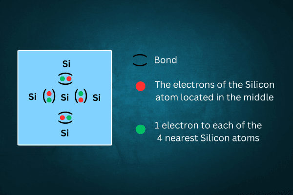
Each electron forms a covalent bond with an electron from the neighboring silicon atom. Thus, the central silicon atom forms 4 covalent bonds with the 4 nearest silicon atoms. In this condition, the number of effective electrons in the outer shell of the atom is 8. These bonded electrons are called valence electrons. Thus, filling the octet stabilizes each crystal atom and keeps the crystal in balanced bonds.
At absolute zero, i.e. 0 K temperature, every electron in the crystal is bound; Since no free electrons or holes exist, no current flows through the crystal, i.e. the crystal behaves like an insulator.
Conduction electron
As the temperature of the semiconductor crystal increases, i.e. the crystal absorbs heat, the energy of its conduction electrons increases. As a result, at least some of the electrons gain enough kinetic energy to break the covalent bond and escape. These debonded electrons are free electrons, which act as charge carriers in the crystal. Applying a suitable potential difference allows these electrons to conduct current in the Silicon or Germanium crystal. These charge carrier-free electrons are also known as thermal electrons.
Incidentally, the conductivity of a substance is proportional to its free electron concentration n. n ≈ 1023 m-3 for good conductors and n ≈ 107 m-3 for insulators. For semiconductors, the value of n lies between these two values. For example, at 300 K, i.e. room temperature, the values of n for germanium and silicon are n ≈ 1019 m-3 and n ≈ 1016 m-3 respectively.
Flow Value: The current through a pure Germanium crystal does not exceed a few microamperes or µA (10-6 A). For Silicon, this current value is even lower, only a few nanoamperes or nA (10-9 A). Such low currents are of no practical use, so pure semiconductors have no use as electrical materials.
Resistance of Semiconductors: As the temperature of the Silicon or Germanium crystal increases, the number of free electrons inside it also increases. As a result, the current flow also increases, i.e., the resistance of the crystal decreases. On the other hand, we know that the resistance of metallic conductors increases with increasing temperature.
Hole
Origin of hole: Suppose, in a pure Silicon crystal, the electron in the A position of the 1st bond breaks the covalent bond and moves to the X position. That is, a valence electron is converted into a conduction electron. Immediately there is a deficiency of an electron in the A position, that is, there is no more electron in that position. Hence, an effective positive charge arises at position A relative to the surrounding electron assembly. This lack of electrons in the bond is known as a hole. If the charge of an electron is -e, the effective charge of the hole is +e. Note that in a pure semiconductor, exactly as many holes are created as electrons are liberated, i.e. n = p (where n and p, are the concentration of electrons and holes respectively).
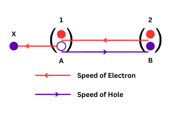
Velocity of hole: Now suppose that a potential difference is applied between the two ends of the said crystal. The electron in the B position of the 2nd bond breaks the bond and escapes due to thermal vibration. Now, due to the applied potential difference, this electron moves in a certain direction and finally fills the vacancy at the A position of the 1st bond. Immediately the hole at position A will disappear and a new hole will appear at position B. It can be assumed that the hole at position A is moved to position B. Obviously, holes move in the opposite direction to the electron moving through the crystal. Remember, a hole is not a real particle, just an ‘electron deficiency’. Nevertheless, it is often convenient to describe current flow in terms of hole speed; That is why in a Silicon or Germanium crystal electrons are assumed to be negative charge carriers and holes are also assumed to be positive charge carriers.
Definition: When an electron is separated from the bond of an atom, the vacancy created at that position is called a hole. Its effective charge is +e, although it is not a real particle.
Energy bands in solids
As an example, we can start by discussing the element Sodium (Na) and its atoms. The figure shows an isolated Na atom, with atomic number Z = 11 and electron configuration 1s22s22p63s1. The attraction by the nucleus creates a potential well and the electrons reside in different isolated and negative energy levels within this potential well. According to Pauli’s exclusion principle, each energy level can have at most two electrons with opposite spin.
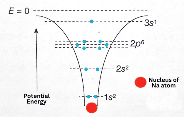
The sodium atom has 2 electrons in the 1s energy level and 2 electrons in the 2s level; The 2p energy level splits into three sublevels, so that level has 6 electrons. The outermost electron is in the 3s energy level—this is the valence electron of the sodium atom.
Then, one can consider several sodium atoms densely packed within the crystal lattice of solid Sodium. Due to this compaction, the shape of the potential well is changed. In general, the electrons except the valence electrons (10 in the case of the Sodium atom) remain in each atom’s potential well, so that the influence of other surrounding atoms on them is negligible.

But an entirely different situation arises in the case of valence electrons. This electron no longer resides in the potential well, so each valence electron can be affected by more than one atom at the same time. In fact, there is no way to indicate which valence electron belongs to which atom. In short, Sodium crystals occupy a large number of electrons in the 3s energy level. However, another problem arises in this case. According to Pauli’s exclusion principle, no isolated energy level can contain more than 2 electrons. As a result, the 3s energy level splits into a number of sub-levels, each with 2 electrons. A crystal can contain 1020 or more atoms within a very short range, so the number of such sublayers is so large that the stability of the layers can be assumed to vary continuously. These energy levels form an energy band at the 3s position; This band is called the valence band of crystalline solids.
In general, each electron in the valence band moves out of its atom but remains under the influence of the attraction of the whole crystal’s atomic mass, i.e., the remaining ionized atoms. Consequently, no valence electrons behave like free electrons i.e., they are not available as charge carriers for the flow of electricity.
Now, if the valence electron somehow gains energy from the outside and can move beyond the influence of the crystal’s atomic aggregation, it becomes a conduction electron. When a potential difference is applied between the two ends of the solid, the conduction electrons are deflected, resulting in the generation of electric current in the solid. Again, many valence electrons can simultaneously gain energy to become conduction electrons, so they also form energy bands rather than being in a single isolated energy level. This is called a conduction band.
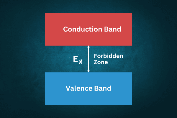
Naturally, the electrons in the conduction band are more energetic than the electrons in the conduction band. Between these two bands is a forbidden region—no electrons can exist in this region; The energy gap between the two bands is called the forbidden energy gap and is denoted by the symbol Eg. This energy gap is different for different materials and depending on it the electrical conductivity of different materials is also different.
Insulators: In materials where the energy gap between the valence band and the conduction band is very large, the conduction electrons rarely attain enough energy to become conduction electrons. As a result, no charge carriers are formed and the material behaves as an insulator. In this case, Eg > 3 eV.

Conductors: In some materials, the top of the compatibility band and the bottom of the transport band end have overlapped. That is, Eg = 0. As a result, valence electrons can become conduction electrons almost effortlessly. Hence, a lot of charge carriers are formed and the material behaves as a good conductor.
Semiconductors: Materials that have a small energy gap between the valence band and the conduction band, behave as semiconductors. This is because the energy required to convert valence electrons into conduction electrons is much higher than that of conducting materials. However, in semiconductors, the energy gap between the valence band and the conduction band is not as insurmountable as in insulating materials. This energy gap is 0.67 eV and 1.11 eV for Germanium and Silicon respectively. This value is called the thickness of the potential barrier between the valence band and the conduction band. Electrons can move from the valence band to the conduction band only when a potential difference of at least 0.67 eV for Germanium and 1.11 eV for Silicon is applied. As a result, electron-hole pairs can be formed.
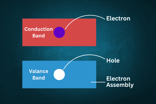
Origin of hole: At low temperatures, the valence band of a pure semiconductor is in a saturated state and the conduction band is in an empty state. Now at higher temperatures, whenever an electron reaches the conduction band from the valence band, an electron vacancy is created at one of the positions of the valence band, i.e., a hole is created. The number of electrons in the conduction band of a pure semiconductor is equal to the number of holes in the valence band.

Pingback: Impure or extrinsic semiconductor - ASTRONOMY ADVENTURE
Pingback: Zener diode - ASTRONOMY ADVENTURE
Pingback: Transistor - ASTRONOMY ADVENTURE