p-n Junction
Definition: When one part of a semiconductor crystal is p-type and the other n-type by reverse doping, the crystal is called a p-n junction.
A p-n junction is shown in the figure. There is a junction between the p-type part and the n-type part. Incidentally, p-n junctions are not formed across two separate p-type and n-type crystals; Because no matter how well coupled, the interface becomes permeable to electrons and holes. Therefore, a single crystal is p-type doped in one part and n-type doped in the other. Connections made in this way do not have an obvious interface. But it is possible to make the interface as narrow as 10-6 m. For convenience of discussion, the connection is assumed to be an ideal connection. That is, there is a clear interface between the p-type and n-type parts.

Circuit symbol

The circuit symbol by which p-n junction is represented is shown in figure. The base of the inscribed triangle points to the p-end; The point parallel to the base drawn at the vertex indicates the n-end.
Depletion zone or depletion layer
As soon as a p-n junction is formed, electrons and holes flow through the intersection. But let’s see what the connection is like before the distribution starts. In this state, the free electrons in the n-type region move around randomly and the donor ions are locked in their respective positions. Since the free electrons are confined to the n-type region, the total charge of the n-type region is zero. On the other hand, in the p-type region, the free holes move around randomly and the acceptor ions are firmly locked in their respective positions. Since the free holes are confined to the p-type region, the total charge of the p-type region is also zero.

Both n-type and p-type parts have zero charge. As free electrons do not exist in the p-type region, the free electrons start crossing the junction into the p-type region. Again, the free holes begin to cross the junction into the n-type region due to the non-existence of free holes in the n-type region. That is, the circulation begins. Electrons move to the p-type region due to diffusion quench holes in acceptor ions near the junction. As a result, the acceptor ions become negatively charged, i.e., the total charge of the p-type portion. Similarly, holes transferred to the n-type region as a result of diffusion quench the electrons of the donor ions near the junction. As a result, the donor ions become negatively charged, i.e., the total charge of the n-type portion becomes negative.

As a result of the diffusion process, the n-type and p-type parts gradually increase in the amount of positive and negative charges respectively. At some point, this charge becomes so great that no electrons or holes can cross the junction to the other side, i.e., the net diffusion is zero. In this case, no free charge exists over a small region on either side of the interface. This zone is called the depletion region.

Negative ions are present in the p-type part and positive ions in the n-type part of this depletion region. That is, the higher potential of the n part can be considered as a potential barrier at the p-n junction for the lower potential of the p part. The majority of carriers, electrons, or holes cannot cross this barrier.
However, even after the formation of a potential barrier, the movement of minority carriers is maintained. Since the depletion region has a positive potential towards the n part, the minority electrons in the depletion region of the p part are attracted towards it; Again, the minority holes located in the depletion region of the n part are attracted towards the depletion region of the p part with negative potential. Hence, the minority carriers in the depletion region are also in motion.
Application of forward and reverse bias to p-n junction
Applying a bias is to connect a device such as a diode, transistor, etc. to an external current source (e.g., a battery).
Application of forward bias
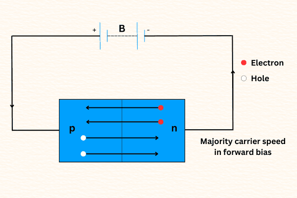
To forward bias a p-n junction, an external current source (B) is connected to the positive terminal of the p-terminal and the negative terminal of the n-terminal to the negative terminal. Part of the applied forward bias is used to reduce the potential barrier value. To reduce the height of the potential barrier, the value of the applied voltage should be increased. Thus, when the applied voltage reaches a certain value, the potential barrier height becomes zero. At this time, the depletion region disappears. If the value of forward bias is further increased, holes in the p region and electrons in the n region can easily cross the interface. That is, the positive potential applied at the p end and the negative potential applied at the n end help the holes and electrons to cross the interface respectively. This results in the flow of current in the external circuit. According to conventional wisdom, the direction of flow in the external circuit is opposite to that of electron flow, i.e., the direction of hole flow.

Application of reverse bias
Reverse bias is applied to the p-n junction by connecting the n-end to the positive terminal and the p-end to the negative terminal of the external current source (B). The depletion region expands further when a reverse bias is applied. As a result, there is no movement of mass electrons and holes across the interface, and no current is obtained in the external circuit.
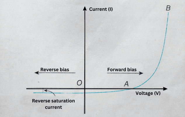
However, little flow is obtained for minority carrier motion; Its value is about 10-6 A in germanium, and only 10-9 A in silicon. This current is called the reverse saturation current of the diode. In most cases, this flow is ignored.

Note that before any external bias is applied, the p-side becomes negative and the n-side becomes positive for diffusion and a depletion region hence a potential barrier is formed on either side of the junction. This is called natural reverse bias.
Semiconductor diode
Applying forward bias to a p-n junction causes current to flow through it, but applying reverse bias stops the flow. So, the p-n junction behaves like a valve, i.e., the flow through it is unidirectional. A p-n junction is also called a semiconductor diode. A p-n junction can be used instead of a vacuum diode as an alternating current rectifier.
Characteristics curve of p-n junction diode
The variation of current with applied voltage across a p-n junction diode for forward bias and reverse bias is shown in Fig. This is called the ampere-volt characteristic curve or the I-V characteristic curve of the p-n junction.

Characteristics curve of p-n junction diode
- A reverse bias current exists for minority carriers.
- A minimum forward bias is required to disable the associated reverse current.
- As the forward bias increases further, the current increases very rapidly.
- The characteristic curve of the p-n junction is not linear, i.e., V and I are not proportional to each other. Hence, it is a non-ohmic electrical element. If the change in current is ΔI for a change in voltage ΔV, the ratio ΔV/ΔI is called the dynamic resistance of the junction. The value of this dynamic resistance rp is different in different regions of the characteristic curve.
p-n junction rectifier
A device that converts a sine wave into a unidirectional waveform or a bidirectional current into a unidirectional current is called a rectifier. A p-n junction diode is used for rectification of alternating current.
Advantages of silicon over germanium
Even in the case of reverse bias for minority charge carriers small current is obtained through the p-n junction. Hence p-n junction diode as a rectifier is not completely error-free. The value of this reverse current is about 10-6 A in germanium, but only 10-9 A in silicon. This reverse flow is easily ignored in silicon. Therefore, silicon is more suitable than germanium as a rectifier.


Pingback: Binary System - ASTRONOMY ADVENTURE